Micro-via advantages in multi-layer PCB’s
- Shorter trace lengths
- Fewer signal layers – due to shorter trace lengths
- Enhanced RF-capability – due to same
- Improved EMC-characteristics – due to same
- More room for components – often two sided assembly can be avoided
- Much more room for components with R7011 build
- Smaller pcb for same functions possible
- Micro via technology have better reliability than through holes
- Integration of screen resistors resistors on layers 2 and n-1 is feasible
- Reduction of drilled through-holes
- Environmentally friendly
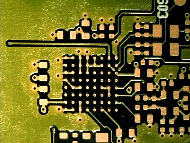 BGA Contacts 64_Pitch 0,8_Pad 0,3_Line/Space 0,15_Vias 0,3_Microvias 0,1 mm
 UV-Jag laser drilled in RCC-folie 0,1mm and stepped 0,2 to 0,1 mm
